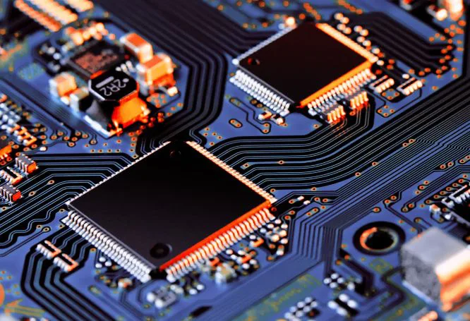
Semiconductor industry is soaked with one of the most ever-advancing technologies. The demand for smaller, faster, and more efficient microchips keeps the world of semiconductors on its toes.
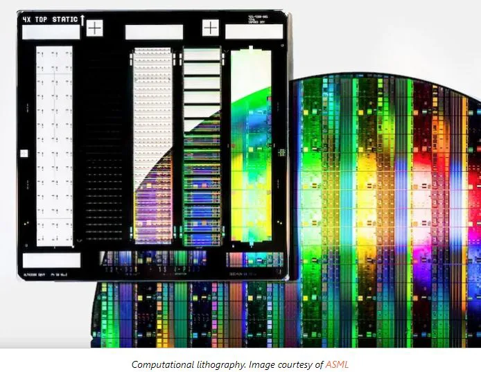
Computational lithography has totally revolutionized the field by meeting the desired level of precision and complexity in chip design.
By leveraging the power of computational algorithms and advanced mathematical models, computational lithography has become an indispensable tool in the creation of next-generation chips.
The progression of lithography
To understand the significance of computational lithography, let’s first try to understand the concept of traditional lithography.
Lithography, in chip manufacturing, is a technique of transferring a desired pattern onto a silicon wafer using light and a mask.
The advancement of technology is inversely proportional to the chip size. This implies that as technology moves to higher levels, the size of the chip starts to shrink to nanometer scales. Thus, it becomes an apparent limitation on the shoulders of traditional lithography.
The wavelength of light used in lithography becomes a bottleneck. This led to diffraction and reduced resolution.
Enter computational lithography
So, to counteract this problem, computational lithography took center stage. Very deftly, it disabled the limitations of traditional lithography. Like a rookie, it became a paradigm shift that combined the power of:
- mathematics
- physics
- computer science
With the help of sophisticated algorithms and simulations, computational lithography optimizes the process, enhances resolution, and achieves unprecedented precision.
By playing around with complex interactions between light and matter, the technique allows chip designers to push the boundaries of what is physically achievable.
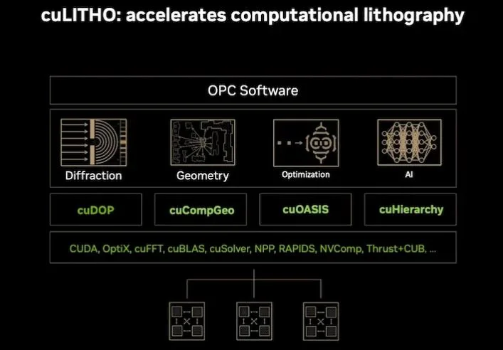
To address the demands of computational requirements for algorithmic modelling, NVIDIA has already come up with cuLitho – a software library for computational lithography.

Computational lithography sustaining Moore’s Law
Gordon Moore, in 1965, stated that the number of transistors on a microchip will double nearly every two years. Since then, this phenomenon has been the driving force behind the rapid advancement of technology.
Meanwhile, there is a limitation to nearly everything; traditional lithography too fell into the clutches of physical limits. It threatened the sustainability of Moore’s Law.
However, computational lithography allows chip designers to pack in more transistors while continuing the downsizing of component dimensions.
Thus, the technology ensures that the industry could sustain Moore’s Law for the foreseeable future.
Computational algorithms mean “following the light”
Advanced algorithms are the key players that form the foundational stones for the success of computational lithography.
How?
Well, the microchips have super intricate layers. The “advanced algorithms” can mimic how light moves through all those layers.
Algorithms include some calculations that can help in figuring out the best design for the mask that creates the patterns we want on the chip.
It’s like they’re playing a virtual game of “follow the light” to make sure everything turns out just right. Algorithms simulate how light moves through all those complex layers on the chip, just like a player following a path. Ultimately, the process is able to create the desired patterns on the chip.
Machine learning algorithms with computational lithography
To enhance resolution and reduce manufacturing errors, the algorithms also make use of optimization techniques, such as inverse lithography.
Besides, machine learning algorithms have been integrated into the computational lithography workflow. The combination not only enables the system to learn from vast amounts of data, but it also improves its predictions and optimizations over time.
Increasing complexity and challenges
Chip designs are becoming progressively intricate. In the realm of computational lithography, this has surfaced a huge set of challenges. It’s like trying to navigate a labyrinth with a blindfold on.
The interaction of light in these three-dimensional structures is a conundrum that has no easy solution. Furthermore, huge computational resources are required to accurately model and simulate these interactions.
Engineers need to bring about new and improved algorithms, upgrade their hardware, and harness even more computational power. Unlike progress in our reality, their progress is measured in nanometers and milliseconds.
Computational lithography has accelerated tech advancements
No doubt, computational lithography has allowed for the creation of smaller and more powerful chips. Now engineers are equipped to design chips with higher performance, lower power consumption, and improved reliability. This has a direct impact on innovation across various sectors, such as:
- artificial intelligence
- data centers
- mobile devices
- autonomous vehicles
The adoption of computational lithography has not only accelerated technological advancements but has also driven economic growth and competitiveness.
Takeaway
The future of computational lithography looks promising. Its fusion with different cutting-edge technologies will surely create a seismic shift in the world of chip design. Deloitte Global has predicted that the world’s leading semiconductor companies will spend US$300 million on internal and third-party AI tools for designing chips in 2023.
Technologies like extreme ultraviolet (EUV) lithography and nanoscale materials together will form an unstoppable alliance. And unlimited possibilities for chip designers everywhere.
Furthermore, quantum computing, with its mind-bending quantum bits or “qubits,” has the potential to revolutionize chip design in ways we can’t even fathom.
How?
In the world of quantum computing, bits are no longer limited to just 0s and 1s (which happens in classical computing). Each bit can exist in both states simultaneously. If bits can be in multiple places at once, then parallel computations could be a matter-of-fact way.
Computational lithography will be the engineer’s brush with which they will paint/etch intricate patterns of light and matter with unparalleled precision.
The possibilities are limitless, and by merging the tech together, we can unlock a world of groundbreaking advancements beyond our wildest dreams.