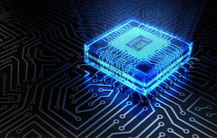
Tech behind computational lithography has revolutionised the way semiconductors are fabricated. By harnessing the power of computer algorithms and simulations, chip designs have become more efficient and powerful than ever before.
Its ability to optimize lithographic processes have given a huge boost to the overall performance and energy efficiency of electronic devices.
As we move forward, computational lithography is expected to merge with other technologies and re-shape the future where technology knows no bounds.
Computational lithography, undoubtedly, is brimming with a plethora of new opportunities. Following are some of the exciting possibilities burgeoning in the field.
AI and Machine Learning enhance Precision in Chip Manufacturing
First thing that comes to our mind is synergizing the power of machine learning algorithms with computational lithography.
The combination will lead to improved accuracy since technology behind optical proximity correction (OPC) and source mask optimization (SMO) will enhance their optimization capabilities.
AI-powered pattern recognition will lead to better lithography performance with reduced manufacturing costs. It’ll be a game-changer that will make everything better and more efficient.
Machine learning models can forecast defects and boost yield. Thus, leading to top-notch, high-quality chips.
With this these kinds of synergies, chip manufactures can ensure smoother and more efficient manufacturing processes. This will also result in better products overall.
Synergies between EUV Lithography and Computational Lithography
In semiconductor manufacturing, DUV lithography (Deep Ultraviolet Lithography) had occupied the center stage for many years. But as technology nodes shrink, EUV lithography (Extreme Ultraviolet Lithography) struts onto the scene with a confidence.
DUV’s wavelength of around 193 nanometers has reached it upper limits. The diffraction limit caused by the relatively large wavelength of the light caused it to go no further.
While EUV light danced at startling 13.5 nanometer wavelength. With this tiny configuration, the light was able to print amazingly small and intricate patterns on silicon wafers.
Now when computational lithography steps in, powered with artificial intelligence and advanced algorithms, the EUV Lithography will result in higher & better resolution, faster processing times, and a whole new level of chip design and complexity.
The effect will surely bring new life to Moore’s Law as well.
The Magic of Nanoimprint and Computational Lithography
Nanoimprint Lithography (NIL) is a tech that creates patterns on a nanoscale level.
In the world of NIL, a mold with the desired pattern is pressed with the help of heat and pressure on a substrate. Once the resist solidifies, the mold is removed, leaving behind the required design.
NIL is a master of tiny details in the most cost-effective manner. Its efficacy increases by quantum leap once it gets integrated with computational lithography techniques.
If computational lithography is the brain, then NIL, is an artist.
Computational lithography can tailor-made blueprints for creating intricate patterns. Like a wizard it can make perfect balance between optimizing exposure parameters. Powered by the magic of computational lithography, NIL can mass-produce the next generation of semiconductor devices.
Direct Write Lithography and Computational Lithography Forge a Limitless Future
Direct Write Lithography (DWL) is an interesting technique that requires no physical mask for creating patterns on a substrate.
Unlike its predecessor, traditional photolithography, which required mask for copying the pattern on substrate. Followed by exposure of optical or electron beam, the DWL is devoid of any mold or mask.
DWL allows for direct pattern “writing” on the substrate. A focused electron or ion beam, laser, or any other forms of energy beam is used to manufacture custom patterns. Thus, the output designs result in high resolution and complex architectures.
Computational lithography when combined can serve as a complementary technology for DWL. Like a guiding star, it will bestow DWL a touch of precision and perfection to the mix.
With that power mix, the integration can speed up the innovation cycle. Faster prototyping and low-volume production will become a matter of ease.
Consequently, catering to niche market with unique needs of specialized devices and applications will become a breeze with their combined powers. From microelectronics to nanotechnology and beyond, the possibilities are limitless.
Unveiling New Materials via Quantum Simulations
The computational prowess of quantum computing will pave the way for new frontiers. Although, many sectors – including pharmaceutical advancements to climate modelling and financial predictions – will undergo a profound transformation, semiconductor manufacturing will stand tall.
The fusion of quantum computing and computational lithography will unleash a symphony of possibilities. With the magic wand of quantum algorithms, the optimization of complex lithographic processes will accelerate.
Like architects of progress, the dynamic duo of quantum computing and computational lithography, will design a future of innovation and wonder.
Quantum simulations will allow researchers to explore new materials. Thus, enabling designers to engineer substances that were once mere figments of the imagination.
Such as lightweight yet incredibly strong materials with astonishing conductive properties that will surely revolutionize electronics. It’ll be like witnessing a symphony of atoms and particles dancing in harmony.
There could also be possibility of blossoming novel lithographic methods. The possibilities are limitless.
Custom-designed chips and IoT devices
As we step into future, Internet of Things (IoT), might become a lifestyle necessity. Our personal world would then be mesh of vast web of smart devices, where communication and sharing data across gadgets will be at astounding speed.
To make the network convenient, a new breed of semiconductor devices would act as a game changer. Here, computational lithography would be the catalyst to make these IoT dreams come true.
The tech will make personalized IoT chips for everyone. Computational lithography has the power to mold and shape the semiconductor devices with unparalleled precision. Consequently, bringing forth chips that perfectly align with the diverse demands of the IoT universe.
Custom-designed chips will enable a world where the Internet of Things thrives like never before.
Future of High-Speed Data Communication and Processing at the Speed of Light
Photonic Integrated Circuits (PICs) have already captivated the audience. PICs enable high-speed data communication and processing, at the speed of light.
The photonic integrated circuit (PIC) global systems market will grow to US$19.7 billion by 2033, with most of this coming via communications applications, which are valued at US$16 billion by 2033.
Like a compass, computational lithography will lead designers through the labyrinth of intricate designs and manufacturing challenges. And consequently, ensuring the success of these extraordinary PICs.
From lightning-fast data transfers to cutting-edge processing capabilities, we will witness a a world of high-speed data communication and processing.
Takeaway
Computational lithography will continue to evolve. Its light that shines on the world of microelectronics and nanotechnology seems brighter than ever before.
Its integration with emerging technologies will definitely propel semiconductor manufacturing to new heights.
As we venture forth, the line between science fiction and reality blurs. And this unlocks the true potential of technology to better humanity. Welcome to the age of boundless innovation and the dawn of a new era.
