
Physicists and engineers have been working on quantum technologies, like quantum microscopes, for years. The tool enables for in-depth study of the properties of quantum particles and states.
Recently, a team from SQC/UNSW Sydney and the University of Melbourne has developed a solid-state quantum microscope. The microscope can manipulate and analyse atomic qubits in silicon.
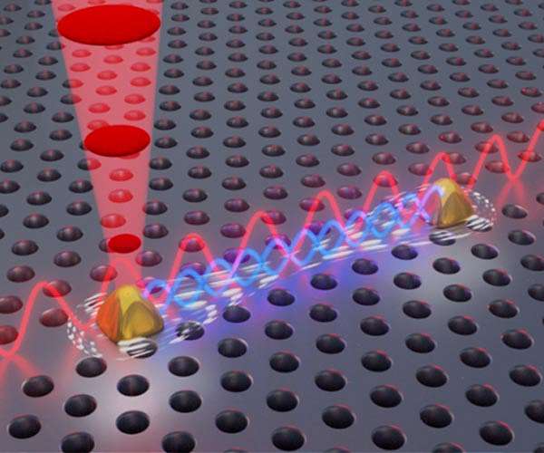
They combined ion implantation and atomic precision lithography techniques to create this microscope.
Ion implantation involves implanting high-energy ions into a material, such as silicon. The process is done by accelerating ions and directing them onto the surface of the target material.
This implantation process can modify the material’s properties, such as its conductivity or doping level, by introducing impurities or altering its crystal lattice structure.
Atomic precision lithography, on the other hand, is a fabrication technique used to create patterns with extremely high precision at the atomic or molecular scale.
The process is done by manipulating individual atoms or molecules to position them in a specific arrangement on a surface.
By putting them on precise placements, it allows for creating intricate structures. This further helps in controlling over their properties and functionality.
Significance of Electron Spatial Distribution
Physicists Benoit Voisin and Sven Rogge highlighted the importance of understanding the spatial distribution of electrons. A complete knowledge of how the electrons is distributed in terms of their positions and densities in three-dimensional space, corresponds to the wave functions of qubits in quantum devices
Manipulating and overlapping these wave functions is crucial for efficient quantum circuit construction.
Spatial Extent of Quantum States with Scanning Tunneling Microscope (STM)
Wave function spatial information is usually unavailable during qubit device measurements, which rely on fixed charge sensing of the overall quantum state.
However, a scanning tunneling microscope (STM) provides direct access to the complete spatial extent of the quantum state.
The team has developed an STM capable of precise atom placement in silicon. Therefore, the research had combined local wave function control for device operation directly within the microscope.
Unifying Qubit Device Manufacturing and Scanning Tunneling Microscopy
Previously, the lab at SQC/UNSW Sydney had been engaged in manufacturing qubit devices and creating scanning tunneling microscopes for imaging qubit wave functions. Their focus was on using individual phosphorus atoms within silicon.
However, in their recent paper, researchers including Voisin and Rogge aimed to combine these separate research endeavors into a unified platform.
Their objective was to develop a quantum microscope capable of both mapping and controlling atomic qubits, utilizing local electrodes within a single device.

Solid-state Quantum Microscope is like a Transistor
Voisin and Rogge described a quantum microscope as a tool capable of engineering arrays of atoms with atomic precision.
Each atom, or qubit, can be controlled and measured locally.
They compared their solid-state quantum microscope to a transistor, with local electrodes defining the source and gate sides.
The scanning tunneling microscope (STM) tip acts as a drain, which can move with extremely high resolution from one qubit to another, scanning their wave functions in the process.
Quantum Microscope Developed through Innovative Fabrication Methods
The researchers combined two techniques, atomic precision lithography and ion implantation, to create their new quantum microscope.
This innovative fabrication method was developed at UNSW. They used atomic precision lithography to introduce dopant atoms and ion implantation to create the electrodes for their device.
The qubits were defined using atomic precision manufacturing, where a few phosphorus atoms were incorporated into hydrogen patches on the silicon surface near the source electrode.
Unlike typical STM experiments on conductive substrates, the microscope operated on insulating silicon.
To map out the qubit wave functions, a light-assisted protocol was designed to first stabilize the STM tip.
Quantum Microscope Utilizes Movable Electrode for Enhanced Qubit Array Measurements
The researchers’ microscope leverages the STM tip as a movable electrode, offering advantages for collecting large qubit array measurements.
This simplifies the process by eliminating the need for multiple fixed sensors, enabling measurements of entire arrays with a single STM tip.
Mapping out qubit wave functions during device operation provides valuable insights for optimizing device design as scaling occurs.
The microscope’s capabilities help speed up manufacturing cycles and enhance device performance in the production of complete circuits using engineered atomic qubits.
Takeaway
Overall, the integration of atomic precision lithography and ion implantation, which are typically separate processes, into a single device marks a significant achievement.
The study by Voisin, Rogge, and colleagues introduces a new approach for fabricating quantum microscopes, potentially sparking innovation in the field of STM and quantum microscopy.
The proposed approach could be extended to microscopes based on other solid-state systems, including molecules and magnetic atoms.