Two-dimensional (2D) semiconductors hold enormous potential to transform the future of electronics. However, their full potential is hindered by a major challenge: interface defects that form between the semiconductors and insulating layers, which degrade overall performance.
To make things clear, let’s take an example of a portable fan that runs on batteries. If the wires connecting the batteries to the fan have a lot of twists or knots or even tiny breaks, the fan will not work efficiently. Similarly, these “twists or breaks” act like traps in a semiconductor. These traps can catch and hold charge carriers, like electrons or holes. Generally, these charge carriers move around freely and conduct electricity. But when they get trapped, their movement is restricted, consequently, it lessens the material’s conductivity and affect its overall performance.
So, what could be the solution?
- Firstly, for the fan to work properly, we need to replace the worn-out wire with a different type of wire that is smoother and more reliable.
- Secondly, we also need to switch batteries to ones that fit better with less resistance. This analogy is quite like the metal gate electrodes in transistors. This component controls how electricity flows through a device, allowing it to function properly.
Now, the current breakthrough shows that using specific metals as electrodes can:
- Significantly reduce leakage current
- Improve the insulating properties of these ultra-thin materials
Thus, bringing us a step closer to develop robust transistors with 2D semiconductors at their core.
Enhanced 2D Semiconductor Transistors
In a collaborative effort of researchers at King Abdullah University of Science and Technology (KAUST), Soochow University and similar institutes have unveiled a new approach that could take 2D semiconductors to the next level in transistor performance.
Their concept involves using hexagonal boron nitride (h-BN) as a dielectric material paired with metal gate electrodes known for their high cohesive energy.
- Hexagonal Boron Nitride (h-BN) as a Dielectric Material: It will insulate and separate different components of a transistor. This dielectric material has not only excellent insulating properties, but it can also create a smooth, defect-free interface with 2D semiconductors. This property will counteract the leakage current, thus improving the overall performance of the transistor.
- Metal Gate Electrodes with High Cohesive Energy: Metals with high cohesive energy are very stable and resistant to wear and tear. Thus, the gate electrodes will remain effective and reliable over time. This will enhance the experience and reduce problems that might arise from less stable materials.
Together, these elements work to create a more efficient and reliable transistor by improving insulation and stability.

Fabrication and Testing of Enhanced Transistors
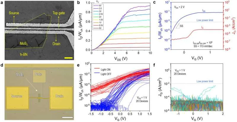
Yaqing Shen, Prof. Mario Lanza, and their team created over 1,000 devices using chemical vapor deposited h-BN as the dielectric material. Upon testing these devices, they discovered that h-BN gate dielectrics worked best with metals that have high cohesive energy, like platinum (Pt) and tungsten (W).
To create transistors with a vertical Pt/h-BN/MoS2 structure, they first cleaned a SiO2/Si substrate using ultrasonic baths with acetone, alcohol, and deionized water. Then following steps were followed:
- Patterned the source and drain electrodes (Ti/Au) on the substrate using electron beam lithography and deposited them via e-beam deposition.
- Exfoliated MoS2 from a natural crystal and transferred it onto the electrodes to form the channel.
- Transferred a CVD-grown h-BN film over the structure using a wet transfer method.
As the final step in their transistor fabrication process, the team:
- Patterned the Pt gate electrode using electron beam lithography.
- Deposited the Pt gate electrode using e-beam evaporation.
- Ensured a clean van der Waals interface between MoS2 and h-BN.
The process improved transistor reliability and performance by minimizing defects and enhancing gate control.
Takeaway
Preliminary tests showed that gate electrodes made of platinum (Pt) and tungsten (W) reduced leakage current through h-BN dielectrics by about 500 times compared to transistors with gold (Au) electrodes. This is a significant improvement with Pt and W versus Au electrodes. Thus, the approach taken by team to develop 2D semiconductor-based transistors so far looks promising.
Therefore, future implications of this research are quite significant. Firstly, with reduced leakage currents and high dielectric strength advanced transistors could be made which will be faster, more reliable, and more energy-efficient, benefiting a wide range of electronic devices.
Secondly, the innovative transistors will be smaller, thus, it’ll push forward the miniaturization trend in technology.
Thirdly, Pt and W-based electrodes in conjunction with h-BN dielectrics will add to the breakthroughs in computing power and electronics. This would lay groundwork for the emerging field of quantum computing.
Over all, the tech will lead to significant progress in electronics and semiconductor technology, influencing both existing and future technologies.
More information: Yaqing Shen et al, Two-dimensional-materials-based transistors using hexagonal boron nitride dielectrics and metal gate electrodes with high cohesive energy. Nature Electronics (2024). DOI: 10.1038/s41928-024-01233-w
Via: Techxplore


