When it comes to data-heavy applications and sustainable computing, photonic chips have emerged as a promising technology. The use of photonic circuits, powered by laser light, offers an edge over traditional electronic circuits. Some of its remarkable advantages over electronic circuits are:
Speed of light: Photonic chips make use of light to transmit and process information, which of course happens at the “speed of light”. Thus, leveraging the feature of light makes them move faster than electrons in electronic circuits.
Therefore, the speed enables faster data transfer rates and reduces latency. This makes photonic chips highly suitable for applications that require high-performance computing, such as artificial intelligence (AI) and big data analytics.
Energy efficiency: Photonic circuits consume significantly less energy compared to electronic circuits.
Electrons while shuttling in electronic circuits, encounter resistance. This results in energy loss and heat generation. On the other hand, photons in photonic circuits flow without losing energy. And so, generating minimal heat.
This inherent energy efficiency makes photonic chips an attractive solution for reducing power consumption in data centers and other energy-intensive computing environments.
Heat reduction: Since, there is no loss of energy in photonic circuits, the need for complex cooling systems to manage heat dissipation becomes redundant. This happens to be one of the major concerns in electronic circuits.
By generating minimal heat, photonic chips alleviate thermal management challenges and contribute to more sustainable computing infrastructure.
Scalability and integration: Photonic chips can be integrated with electronic circuits. With the hybrid systems, benefits of both technologies can be taken.
The integration will enable seamless communication between photonic and electronic components. Thus, it will allow for efficient and versatile computing systems.
Potential for sustainable computing: The energy efficiency and heat reduction offered by photonic circuits make them a promising solution for sustainable computing.
This will also contribute to lower carbon footprints and more environmentally friendly computing practices.
While photonic chips hold great promise, but their widespread adoption and integration into existing computing architectures still face technological challenges.
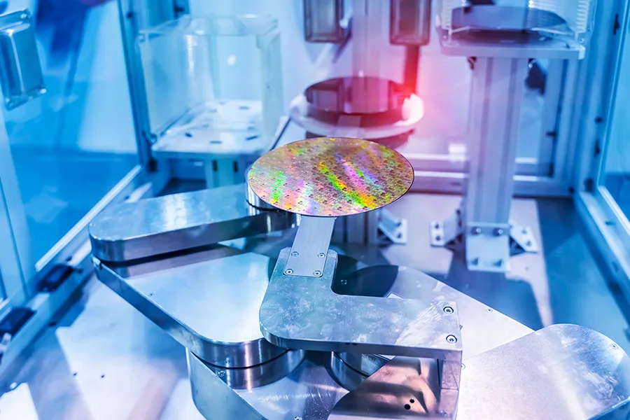
Photonic and electronic circuits both rely on lithography
Photonic and electronic technologies are based on different scientific principles and have distinct architectural structures. However, they both rely on lithography as a common manufacturing technique to define circuit elements and create interconnected pathways.
For instance, transistors form the building blocks of electronic circuits. And lithography is primarily used to fabricate them. With the help of lithographic patterning techniques, the transistors are etched onto semiconductor materials.
While, transistors do not form the fundamental components in photonic chips. Instead, lithography is employed to create complex patterns that guide laser beams through a coherent circuit, forming a photonic network.
These patterns define the waveguides, modulators, detectors, and other optical elements necessary for the manipulation and transmission of light signals.
While the underlying principles and components differ between electronic and photonic chips, lithography plays a crucial role in both technologies. Like an instrument, the technique helps in fabricating the necessary circuit elements and interconnections in both.
Lithographic patterning might get a back seat
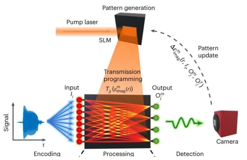
Interestingly, researchers at the University of Pennsylvania School of Engineering and Applied Science, have developed a photonic device that enables programmable on-chip information processing without lithography.
Conventionally, lithography allowed for precise control over the arrangement of optical components and the creation of well-defined pathways for light.
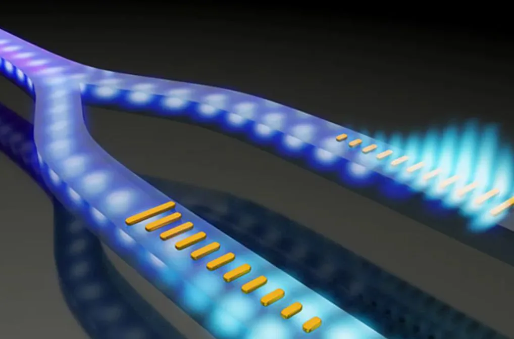
But now, the revolutionary tech has eliminated the need for lithographic patterning. The approach utilizes spatially distributed optical gain and loss within a semiconductor wafer.
In this new device, lasers can be directly applied to the semiconductor wafer, generating areas of optical gain and loss. The spatial variations in optical properties can be controlled and manipulated to achieve desired functionalities.
By leveraging this approach, researchers were able to showcase programmable on-chip information processing capabilities in a photonic device. The tech was able to perform specific tasks or algorithms without relying on lithographic patterning.
Silicon-based electronic systems have practical limits
Although, conventional silicon-based computing technology did transform the computational landscape, but it has reached to its upper physical limits. Photonics seems to be an alternative solution, particularly for machine learning applications.
- They can be slow in processing signals compared to photonics. Since, electronic systems operate using electrons, which have slower speeds compared to photons.
- They process data one step at a time. Thus, limiting in ability to perform parallel processing. In contrast, photonic systems can exploit the parallel nature of light to perform simultaneous processing. Thus, allowing faster and more efficient computations.
- As the components shrink in size, silicon-based electronic systems face challenges related to heat dissipation, energy consumption, and quantum effects. Photonics offer higher-density integration and miniaturization, as light-based components can be fabricated at smaller scales without facing the same physical limitations.
Nevertheless, the fabrication process involving lithographic patterning is complex as well as expensive.
Additionally, lithography can be prone to errors or damage, which can impact chip performance and reliability.
Taking these issues into consideration, researchers created a new paradigm to overcome these obstacles. They removed the step involving lithography. Without relying on lithography, the chips become highly versatile and free from defects that may arise from the fixed patterning process.
This implies that the new approach allows for improved accuracy, reprogrammability, and the removal of constraints associated with predefined features.
Photonic chip technology enables real-time reconfigurable computing
The simplicity of the device lies in its basic structure. While its functionality is achieved through the manipulation of the material properties of the semiconductor slab.
By projecting lasers into dynamically programmable patterns, the computing functions of the photonic information processor can be reconfigured in real-time. This ultimate reconfigurability is crucial for machine learning and AI applications.
The active nature of the material used in the chip forms the vital feature of this tech.
Unlike conventional photonic chips that rely on passive materials scattering light, the active material in this new approach modifies itself under the influence of the pumping light.
This modification enables the release of energy and increases the amplitude of signals when the signal beam arrives, allowing for efficient optical information processing on-chip.
Drawing a computational network with light on wafers
The analogy used by Feng comparing the technology to a pen for drawing pictures on a blank page illustrates the concept well.
The pumping light serves as the pen, drawing the photonic computational network on an unpatterned semiconductor wafer. The unique aspect is that these beams of light can be drawn and redrawn, enabling the creation of innumerable paths and possibilities for future applications.
Takeaway
Photonics holds great promise as an alternative to silicon-based electronic systems, particularly for machine learning applications.
The tech can address the limitations of electronic systems by enabling faster signal processing, parallel computing, and enhanced miniaturization.
Overcoming the challenges in photonic chip fabrication, such as the limitations of lithography, can unlock the full potential of this technology. And significant promise for AI applications, where data-intensive tasks can benefit from the speed of photonics combined with the accuracy and flexibility offered by this new photonic device.