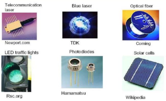
Two-dimensional perovskite materials have unique properties that make them attractive candidates for use in next-generation optoelectronic devices, such as photovoltaic solar cells, LEDs, and photodetectors.
What is a perovskite?
Perovskite materials are a class of compounds that have a specific crystal structure with the formula ABX3.
The most well-known perovskites are metal halide perovskites, where A is a cation such as lead or tin, B is a metal cation such as calcium or nickel, and X is a halogen anion such as chloride or bromide.
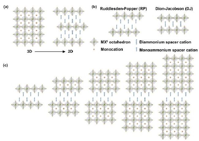
2D perovskites are a subcategory of perovskites with a two-dimensional crystal structure, which offers unique properties, such as
- high photoluminescence efficiency,
- large exciton binding energy, and
- long carrier diffusion length,
thus, making them promising materials for various optoelectronic applications.
2D perovskites as a material for optoelectronic devices
Optoelectronic devices are a class of electronic devices that convert light energy into electrical energy or vice versa. Examples of optoelectronic devices include photovoltaic solar cells, light emitting diodes (LEDs), and photodetectors.
Van der Waals heterostructures integrated from various 2D layered materials are fundamental building blocks for these devices.
The development of 2D perovskites as a material for optoelectronic devices is an emerging field, with continued research aiming to enhance their performance and expand their applications.
Synergistic combination in heterostructure
This expanded potential for functionalities and applications is due to the synergistic combination of the different materials in the heterostructure. For example, the combination of a 2D perovskite with high photoluminescence efficiency and a non-layered material with high electrical conductivity can result in a highly efficient light-emitting device.
The introduction of other 2D materials with distinct properties can also lead to new functionalities, such as improved stability, increased absorption, and enhanced carrier transport.
An overview of 2D/quasi-2D perovskites
Recently, in International Journal of Extreme Manufacturing, researchers at the Huazhong University of Science and Technology have presented an overview of 2D/quasi-2D perovskites and their potential use in heterostructures.
They discussed the structure and physical properties of 2D perovskites and the process of constructing and characterizing 2D perovskite-based heterostructures.
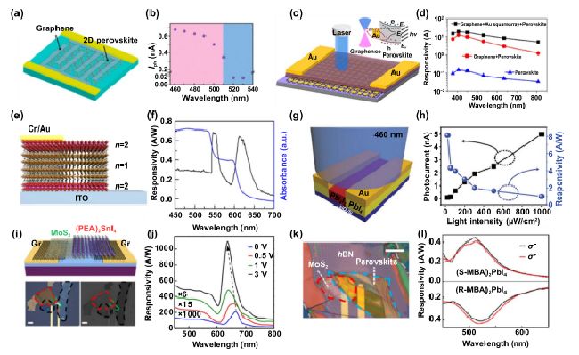
The team also highlighted the unique optical properties of these heterostructures and demonstrated their potential applications in various optoelectronic devices, such as
- photovoltaic devices,
- light emitting devices,
- photodetectors/phototransistors, and
- valleytronic devices.
They also acknowledged the challenges and future perspectives in the field of 2D perovskite-based heterostructures.
Perovskites have rich electronic and optical physics
According to Professor Dehui Li, the lead researcher, 2D perovskites have a rich electronic and optical physics that make them highly promising for optoelectronic applications.
He noted that the electronic structure of 2D perovskites can be effectively modified by changing the layer number, substituting halide anions, and incorporating organic chains, which leads to changes in their optical performance.
However, these modifications can bring both advantages and disadvantages for optoelectronic applications, highlighting the need for further research and development in the field.
2D perovskite heterostructures
The construction of heterostructures lays the foundation for optoelectronic device architecture and applications.
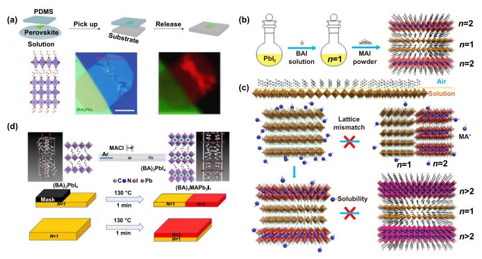
Different techniques have been developed to create 2D perovskite heterostructures, such as dry transfer, solution synthesis, and vapor deposition.
The characterization of the constructed heterostructures is usually done through various methods, including optical spectra, phase identification, and surface morphology characterization.
These techniques provide valuable information about the properties and performance of the heterostructures, which is crucial for optimizing the design and performance of optoelectronic devices based on 2D perovskites.
Optical properties of 2D perovskite heterostructures
According to Dr. Haizhen Wang, who was one of the co-first authors of the study, the optical properties of 2D perovskite-based heterostructures are fascinating and unique. They not only inherit the basic physical properties of 2D perovskites but also exhibit new photophysics that is not present in each individual component material.
This makes 2D perovskite-based heterostructures an ideal platform for studying various processes, such as
- charge/energy transfer,
- ion migration-induced optical properties, and
- nonlinear optical effects.
However, despite these exciting possibilities, research in these areas is still in its early stages and more investigation is needed to fully understand and utilize the potential of 2D perovskite-based heterostructures.
Takeaway
The ability to combine different materials in heterostructures opens a wide range of possibilities for the development of next-generation optoelectronic devices with improved performance and novel functionalities.
The construction of 2D perovskite-based heterostructures with novel functionalities is made possible by the high level of flexibility in the composition, structure, and properties of 2D perovskites.
By combining 2D perovskites with other materials, it is possible to create new heterostructures with unique and improved properties that can be tailored to specific applications in optoelectronics.
The potential for new and innovative device designs is high, and it is likely that the field of 2D perovskite-based heterostructures will continue to expand and evolve in the coming years.