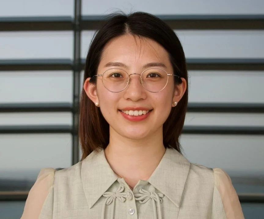
I’m excited to introduce Dr. Yaqing Shen, a highly accomplished scientist in the field of Material Science and Engineering. Her groundbreaking research on advancing the use of two-dimensional (2D) semiconductors in commercial field-effect transistors (FETs) caught my attention. Despite her hectic academic responsibilities, Dr. Shen graciously agreed to an email interview, where she shared insights into her work and career.
Dr. Shen’s journey began during her senior year of college, when a graduation project sparked her passion for experimentation and research. Since then, she has consistently ranked in the top 5% of her field and earned prestigious scholarships—testament to her dedication and expertise.
In our conversation, Dr. Shen discusses how her early industrial career reignited her love for research, and how her drive to explore cutting-edge scientific advancements led her to pursue this fascinating discipline. Despite her numerous achievements, she remains humble and views learning as an endless source of excitement, much like leveling up in a game.
Join me as we dive into Dr. Shen’s inspiring journey of growth, curiosity, and scientific discovery!
How did you get into Material Science and Engineering and what motivated you to pursue it as a career?
My interest in Material Science and Engineering began during my senior year of college when I was required to complete a graduation project. I found the process of investigating and conducting experiments fascinating, especially when analyzing the results and gaining new insights from the data.
After earning my bachelor’s degree, I worked in the industrial sector, but I realized that my true passion lay in research, where I could explore innovative and cutting-edge scientific developments. Inspired by breakthroughs in the field, I decided to pursue a career in Material Science and Engineering, driven by a desire to contribute to advancements in this exciting discipline.
You’ve ranked in the top 5% consistently and earned top scholarships. How do you maintain a mindset of growth and continual learning after reaching such high levels of success?
I don’t consider myself to have reached high success because I am surrounded by many more accomplished people. Additionally, learning new knowledge and skills excites me, much like achieving new levels in a game.
What are the main challenges faced when integrating 2D semiconductors with conventional gate dielectrics? Ref: Two-dimensional-materials-based transistors
The main challenge is that Pt electrodes often have poor adhesion to the substrate during the final fabrication step, which can damage the sample. Before resolving this issue, I encountered many failures and only achieved a few successful devices by chance.
Can you elaborate on the problem of native defects in CVD-grown h-BN and how they affect device performance?
Native defects, such as vacancies, interstitials, dislocations, and grain boundaries, form during the CVD growth process, influenced by various parameters like substrate, nucleation mechanism, growth temperature, and speed. While these defects can be reduced by adjusting these parameters, they are difficult to eliminate completely. Native defects impact the electrical performance of devices and typically occur randomly and unevenly, affecting device-to-device variability.
Could you explain the importance of morphological characterization using atomic force microscopy (AFM) in your research?
Atomic force microscopy (AFM) helps me confirm various parameters of my sample, such as film thickness, surface topography, and phases. This simple characterization method causes no damage to the sample and provides useful and effective information.
What kinds of morphological features are you most interested in when examining 2D materials with AFM, and how do these features correlate with the device’s electrical behavior?
I am interested in the uniformity of 2D materials when measuring with AFM, as several features can affect film uniformity, such as wrinkles, thickness fluctuations, and contamination. These features can impact the performance of electronic devices by causing resistance fluctuations in these areas, which in turn affects variability.
How has the field of memristor technology evolved over the years, and what do you think is the most exciting development in this area?
Memristor technology has advanced from theory to practical use, particularly in non-volatile memory and neuromorphic computing, with its most exciting development being its ability to mimic brain-like synapses for more efficient AI systems.
What do you find most rewarding about working in the field of 2D materials and memristors?
Working in the field of 2D materials and memristors allows me to gain a wide range of knowledge, from the synthesis and characterization of 2D materials to the fabrication of electronic devices and electrical measurements.
What advice would you give to students or early-career researchers who want to explore the intersection of nanotechnology and electronic materials?
1) Develop a clear roadmap for your research, 2) create a feasible plan, and 3) determine the direction for your research career.
Quick bits:
• If you could give one piece of advice on how to develop intelligence—either intellectually or emotionally—what would it be?
Stay open-minded and practice regularly.
• What is your favourite movie quote?
“The people who are crazy enough to think they can change the world are the ones who do.” — Steve Jobs
• Your favourite scientific innovation of the 21st century?
OpenAI
• What will your TED Talk be 10 years from now?
In 10 years, my TED Talk will be “From serendipity to breakthrough: how unexpected discoveries spark major research”.
• If you could solve one global issue, what would it be?
Breaking the limitation of Moore’s law.
• What books should I read in 2024?
Disgust Against Women by Chizuko Ueno
(Wow! Thank you, Dr. Shen, for an incredibly inspiring conversation! Your work is a true source of inspiration. We eagerly anticipate our next visit to witness more of your innovative research. Until then, we extend our best wishes for your continued success in all your future endeavors.)